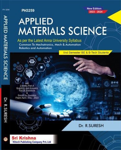
PH3259 APPLIED MATERIALS SCIENCE
SYLLABUS (Regulations – 2021)
Second Semester – B.E. / B.Tech. Degree Course
(Common to Mechanical, Mech & Automation, Robotics & Automation Engineering)
UNIT I CRYSTALLOGRAPHY
Crystal structures: BCC, FCC and HCP – directions and planes – linear and planar densities –
crystal imperfections- edge and screw dislocations – grain and twin boundaries – Burgers
vector and elastic strain energy- Slip systems, plastic deformation of materials –
Polymorphism – phase changes – nucleation and growth – homogeneous and heterogeneous
nucleation.
UNIT II PHASE DIAGRAMS
Phase equilibrium – solubility limit – solid solution (interstitial and substitution) – intermediate
phases – intermetallics – electron compound – Gibbs phase rule – Unary phase diagram (Iron) –
Binary phase diagrams: Isomorphous systems (Cu-Ni) – determination of phase composition
and phase amounts – tie line and lever rule – binary eutectic diagram will no solid solution and
limited solid solution (Pb-Sn) – eutectoid and peritectic reactions – other invariant reactions –
microstructural development during the slow cooling eutectic, hypereutectic and hypoeutectic
compositions.
III ELECTRICAL AND MAGNETIC PROPERTIES OF MATERIALS
Classical free electron theory – Expression for electrical conductivity – Thermal conductivity,
expression – Quantum free electron theory :Tunneling – degenerate states – Fermi- Dirac
statistics – Density of energy states – Electron in periodic potential – Energy bands in solids
– tight binding approximation – Electron effective mass – concept of hole. Magnetic
materials: Dia, para and ferromagnetic effects – paramagnetism in the conduction electrons in
metals – exchange interaction and ferromagnetism – quantum interference devices – GMR
devices.
UNIT IV SEMICONDUCTORS AND TRANSPORT PHYSICS
Intrinsic Semiconductors – Energy band diagram – direct and indirect band gap
semiconductors – Carrier concentration in intrinsic semiconductors – extrinsic
semiconductors – Carrier concentration in N-type & P-type semiconductors – Variation of
carrier concentration with temperature – Carrier transport in Semiconductors: Drift, mobility
and diffusion – Hall effect and devices – Ohmic contacts – Schottky diode.
UNIT V OPTICAL PROPERTIES OF MATERIALS
Classification of optical materials – Optical processes in semiconductors: optical absorption
and emission, charge injection and recombination, optical absorption, loss and gain. Optical
processes in quantum wells – Optoelectronic devices: light detectors and solar cells – light
emitting diode – laser diode – optical processes in organic semiconductor devices –excitonic
state – Electro-optics and nonlinear optics: Modulators and switching devices – plasmonics.








Reviews
There are no reviews yet.